Anti-Static Wafer Pad PS
Product Description: Anti-Static Wafer Pad PS
Product Description
Product Description: Anti-Static Wafer Pad PS
Elevate Your Production with Our Anti-Static Wafer Pad PS
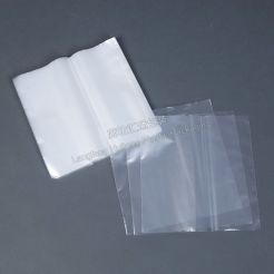
Are you tired of dealing with the costly repercussions of static electricity in your semiconductor manufacturing process? Meet the Anti-Static Wafer Pad PS, your ultimate solution for safeguarding delicate wafers while enhancing efficiency and precision in production. Designed for the modern industry, this innovative pad ensures optimal performance in cleanroom environments.
Key Specifications:
- Material: High-grade polyurethane with anti-static properties
- Thickness: 3mm for optimal cushioning and protection
- Dimensions: Available in standard wafer sizes (150mm, 200mm, 300mm)
- Electrical Resistance:
- Temperature Resistance: Stable performance in a temperature range from -20°C to 80°C
- Surface Finish: Low-friction texture for smooth handling and processing
Prime Advantages:
Link to Tongxi
- Static Protection: Prevent costly ESD (Electrostatic Discharge) damage to wafers, ensuring product integrity throughout handling and transport.
- Durable Construction: Made from robust materials, our wafer pad withstands the rigors of industrial environments without compromising performance.
- Enhanced Handling: The pad's soft, cushioned surface minimizes the risk of chipping and scratching, providing superior protection for valuable semiconductor substrates.
- Versatile Application: Ideal for use in wafer fabrication, assembly, and testing processes, our wafer pad seamlessly integrates into various stages of semiconductor manufacturing.
Unique Selling Points:
- Tailored for Semiconductor Needs: Specifically engineered to meet the stringent requirements of the semiconductor industry, the Anti-Static Wafer Pad PS is a must-have for any cleanroom operation.
- Cost-Effective Solution: By reducing the risk of damage from static electricity during fabrication, our wafer pad helps lower overall production costs and enhances yield.
- Easy Maintenance: The pad is easy to clean and maintain, ensuring longevity and sustained performance in demanding environments.
Applications:The Anti-Static Wafer Pad PS is perfect for a wide array of applications, including:
- Wafer transportation within and between cleanrooms
- Wafer testing and inspection processes
- Assembly lines in semiconductor manufacturing facilities
Customer-Centric Focus:At the heart of our design philosophy is the commitment to customer satisfaction. We understand your challenges and strive to provide solutions that not only meet but exceed your expectations. Investing in our Anti-Static Wafer Pad PS means investing in the security and efficiency of your production line.
Ready to Transform Your Production?Don’t let static electricity compromise your wafer integrity. Order your Anti-Static Wafer Pad PS today and experience the unparalleled protection and performance that will elevate your production standards. Click ‘Add to Cart’ and take the first step towards a more efficient, cost-effective manufacturing process!
Related Products:Anti-Static Wafer Pad PS


